
Nanoelectronics and Optoelectronics for Electronic Nose
In this area, we are exploiting interfacial properties of two-dimensional and one-dimensional interfaces of various heterostructures. Our aim is to fabricate highly sensitive sensing platform for the detection of multiple gases for the air pollution monitoring. In this process we use several algorithms to integrate sensors at room temperature. We were able to successfully integrate sensor for the detection of compressed natural gas (CNG) in collaboration with Gas Authority of India Limited (GAIL). These compact room temperature sensors are applicable to detect leakage of gas in house-hold, manufacturing and storage units, transport pipelines etc. We built a microscopic platform of field effect transistors (FET) for the large array of electronic sensors to mimic neurons in the olfactory system for the detection of multiple gases present in the environment. Machine learning algorithms are implemented for the large data analysis. The laboratory has unique facility to create an environment where molecular detection of various gases is possible upto parts per trillion scale.
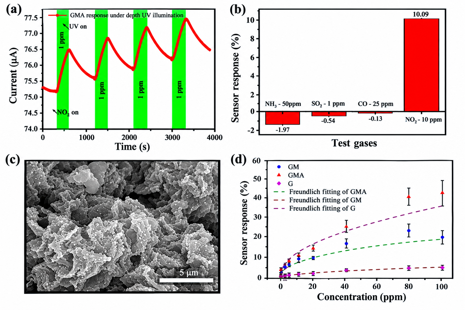
Nanoscale heterojunctions of rGO-MoS2 composites for nitrogen dioxide sensing at room temperature
Figure: Cyclic response of rGO-MoS2-Ag (GMA) towards 1 ppm of NO2 for 4 cycles. (b) Sensor response of GMA towards various test gases at room temperature showing selectivity to NO2.
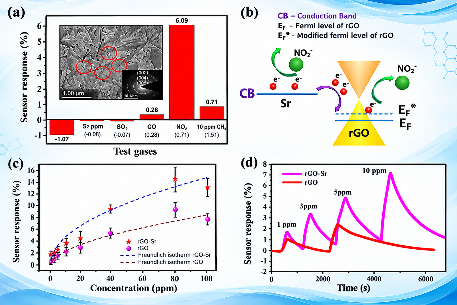
Modified fermi level in strontium nanoparticles decorated reduced graphene oxide for wide concentration detection of nitrogen dioxide at room temperature
Figure: (a) Sensor response of rGO-Sr towards various test gases at room temperature showing selectivity toNO2. (b) Schematic showing the promotion of fermi level in rGO assisted by Sr. Plot of sensor response versus concentration for both the devices. (d) Dynamic sensor response of rGO and rGO-Sr versus time towards varying concentrations of NO2 with UV aided complete desorption.
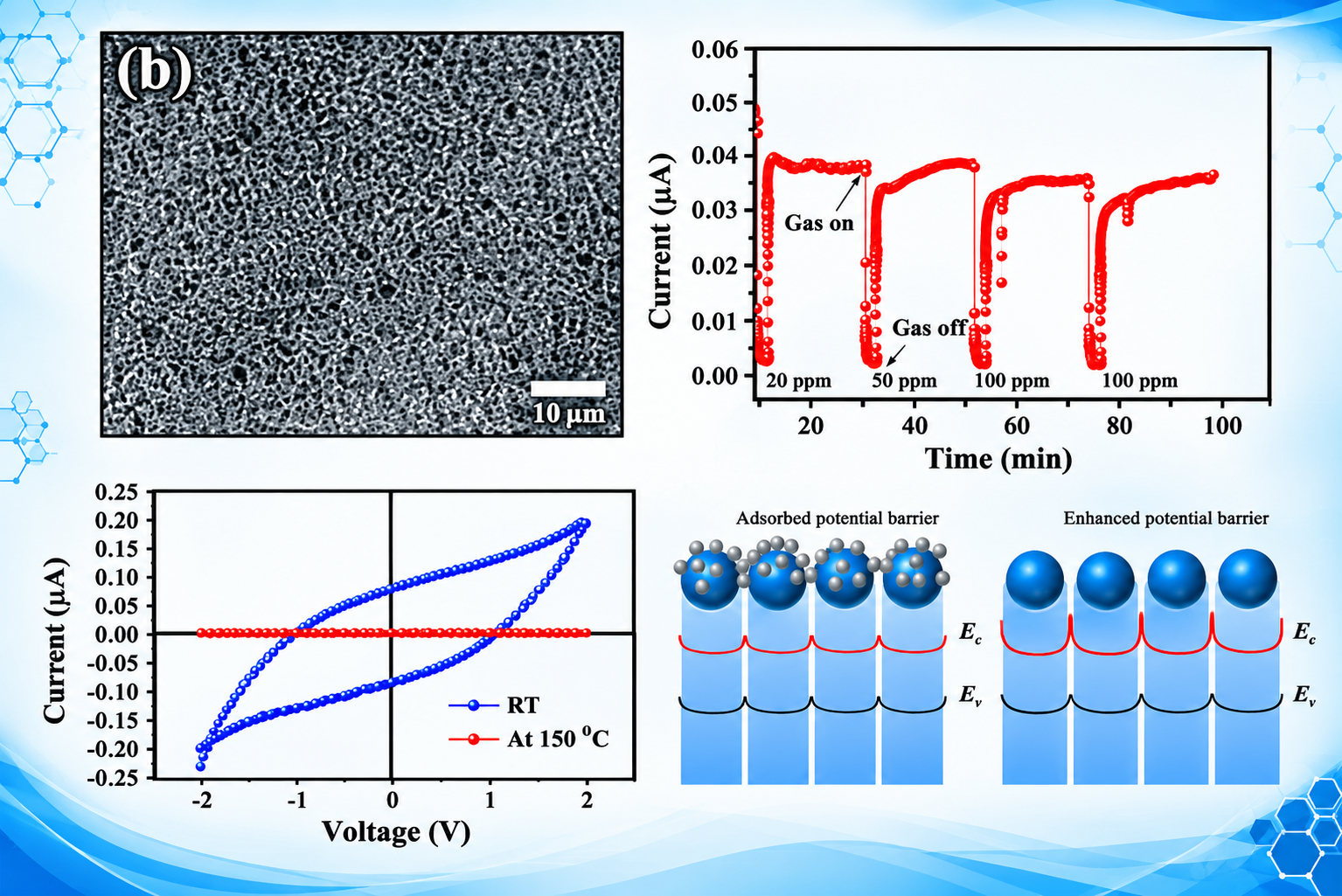
Influence of charge traps in carbon nanodots on gas interaction
Figure: (a) HRTEM image of carbon nanodotss indicating a lattice parameter of 0.18 nm and 0.21 nm. (b) Cyclic response (current) to different concentrations of NO2. (c) I–V measurements obtained by sweeping voltage in the range from ?2 to 2 V in both forward and reverse directions. Measurement curves were obtained at room temperature and at an elevated temperature of 150 °C. (d) Energy band diagram of carbon dots without the presence of water molecules (removal of water molecules either by heat at an elevated temperature or by gas) indicating an enhanced potential barrier for electron flow.
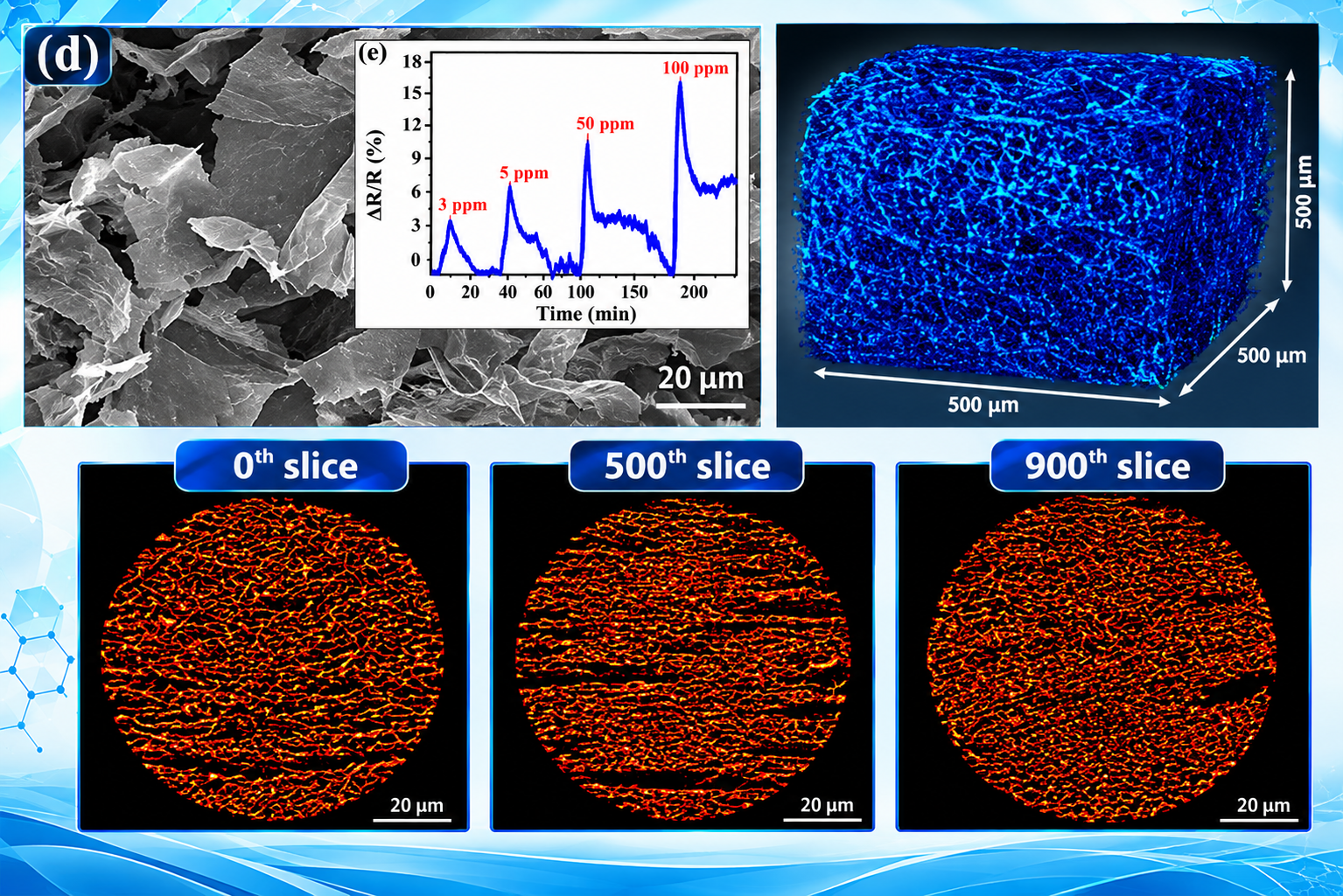
Tailored nitrogen dioxide sensing response of three-dimensional graphene foam
Figure: (a) SEM image of rGO foam, inset shows the NO2 sensing response. (b) Three-dimensional XT micrographs of GO foam. two dimensional images of different slices of the above foam from left to right.
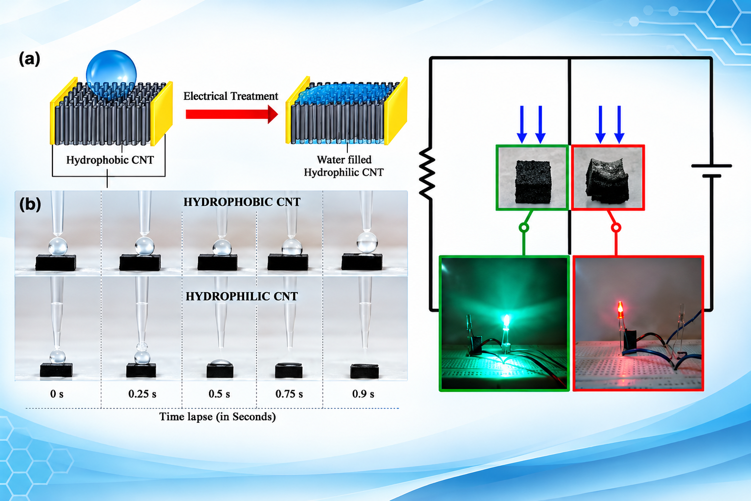
Water-responsive carbon nanotubes for selective detection of toxic gases
Figure: (a) Schematic of the experimental set-up used for converting hydrophobic CNT to hydrophilic. (b) Variation in contact angle of the water drop on both hydrophobic (top) and hydrophilic sample (below) evaluated with the time. In hydrophilic sample, water was confined within the bulk structure, which percolates into the bulk of the forest within a few seconds. Circuit diagram of the proposed gas alarm prototype based on bulk CNT. Green LED glows in the absence of gas and red LED glows after bulk CNT curls up upon exposure to NH3 gas, while eventually breaking a specific part of the circuit.
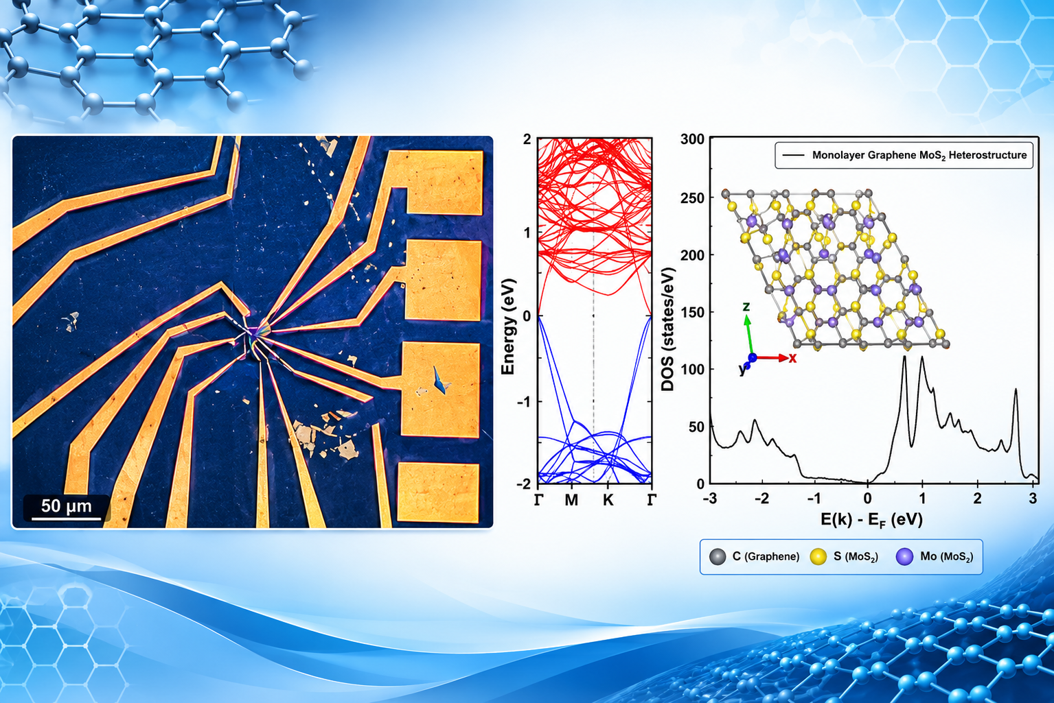
Two-dimensional van der Waals FET devices for NO2 sensing
Two dimensional heterointerfaces are currently being studied for NO2 sensing using field effect transistors.
Figure: (a) Field effect transistor device (b) Density functional theory simulations.
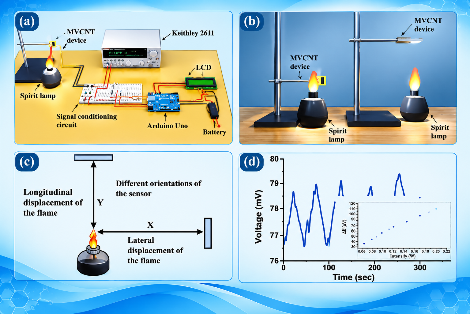
Carbon nanotube based multifunctional flame sensor
(a) Schematic shows the experimental set-up used for sensing flame using MWCNT sensor. (b) and (c) Show the lateral and longitudinal directions of the sensor measurements. (d) Cyclical voltage response of the MWCNT sensor device while applying a fixed bias current and it is exposed to the flame that was kept at 4 cm distance from the sensor in the lateral direction. Reference: Sensors and Actuators B 192 (2014) 594– 600.
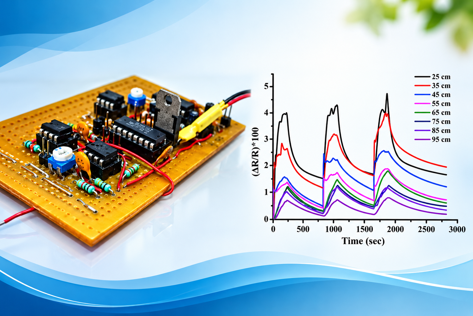
Graphene based multifunctional flame sensor
Circuit setup for the sensor and Variation of normalized resistance change with time on exposure to flame at varying distances of the flame from the sensor vertically.
Reference: Nanotechnology 26 (2015) 195502.
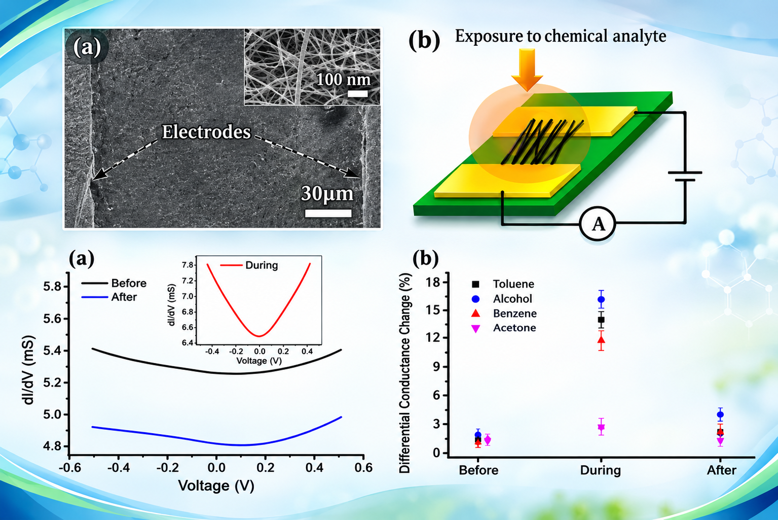
Chemical vapor detection using nonlinear electrical properties of carbon nanotube bundles
Scanning electron microscope image of the CNT dispersed gold electrodes used for the sensing of organic analytes. The inset shows microstructure of the CNT mat in between the electrodes. (b) Schematic of the experimental setup used for the CNT sensor. Differential conductance plotted against bias voltage for ethanol as analyte (before and after analyte exposure). The inset shows the differential conductance plot during the chemical exposure. (b) Percentage-change in differential conductance before, during and after analyte exposure, a comparison of all analytes exposed to the CNT mat.
Reference: Nanotechnology 25 (2014) 025708